An EMC FastPass reader recently asked me what the top EMC design rules were that they could implement on their product to maximize the chances of passing FCC and CE testing. There’s no doubt that there are countless ways to fail emissions and immunity tests, and lack of good EMC design techniques were the problem more often than not.
Regardless of the type of product I was testing, be it medical, industrial, consumer or any other industry for that matter, there were a few areas where manufacturers consistently missed EMC design techniques that could have prevented the failure. Was it possible that EMC failures were distributed according to Pareto’s Law? i.e. 80% of the failures were due to 20% of the cause mechanisms. It seemed possible.
If you want to avoid some of the most common EMC pitfalls, learn some good EMC design tips, and avoid costly re-tests and launch delays, read on…
You might also be interested in:
1. EMC Design Tip #1 – Reduce RF Noise On The Cables
Cables act like antennas for radio noise. One of the top failure modes I saw at the lab were due partly or wholly to EM radiation from the cabling attached to the device under test (DUT).
How good they are at converting the conducted noise to radiated noise (i.e. how good an antenna it is) varies greatly depending on several key factors including the impedance match, the length of the cable and the wavelength of the noise. To avoid radiated emissions issues due to cabling, it’s really important to ensure that as little unintentional noise is coupled on to external and internal cabling as possible.
If a manufacturer runs into a radiated emissions issue at a test lab, one of the first methods of debug is usually to detach as many I/O cables as possible. If the offending emission disappears, then you can start re-connecting the cables one-by-one until you (hopefully) find the culprit. Note that if there are multiple cables, it can very often be the case that each cable contributes towards a particular issue and connecting/disconnecting them in various configurations can lead to seemingly inconsistent measurement results. This is typically due to connecting/disconnecting ground loops of various sizes. Regardless of this, the rule of thumb to keep in mind at the design stage is to keep as much unintended RF energy off every cable as possible.
There are a few EMC design rules that you can use to help minimize the noise emissions from cabling:
(a) Ensure slew rate of signals on the cables are minimized
Digital signals can contain RF energy across a high bandwidth. The upper limit of the bandwidth depends on the slew rate of the rising and falling edges of the signal. The higher the slew rate, the more energy the signal contains at higher frequencies. As you can see from the figure to the right, the RF energy contained within a 1 MHz square wave spans a large spectrum.
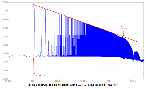
It’s usually possible to reduce the slew rate of digital signals coupled on to cabling by either reducing the drive strength of the driver, or passing the signals through a low-pass filter. By lowering the slew rate, you can greatly reduce the RF energy coupled on to the signals and therefore reduce the amount of radiation from the cabling.
A good ‘get-out-of-jail-free’ design rule is to include a non-populated low-pass filter on every digital signal that passes over a cable. A simple and cheap R-C filter will do the job if your eye diagram can take the hit. Otherwise, more expensive integrated solutions are available. See section 4.2.2 in our EMC design guidelines eBook for more details.
(b) Make sure any power, ground, shield GND and static I/O signals are clean
Although on the surface of it, you’d think that DC signals such as power supplies and static I/O signals should not contribute a significant amount of RF energy to cabling. However, these signals can often be the culprit with cable noise. A global reset signal for instance usually goes to several chips and areas of a PCB. If you’re not careful, this trace can pick up a significant amount of RF noise. When the reset signal traverses a cable, the noise can now be emitted as electromagnetic radiation, sometime causing issues with radiated emission testing.
You could write books on ways to minimize these contributions, and many people a lot smarter than I am, have written many. However, here are a couple of easy to implement EMC design tips that I’ve seen work very effectively at keeping RF noise off cabling.
(i) Add in-line ferrite beads on power supply and static I/O signals
Noise suppression beads are designed to absorb RF energy and convert it to heat. There are thousands to choose from and so it’s worth putting in a bit of time to choose carefully. To over-simplify a complex issue, basically you want the frequency of the peak impedance of the ferrite bead to match the frequency of perceived worst case noise in your circuit so that the energy at that frequency is turned into heat. A fantastic app note that dives into this selection process can be found here.
Even if you decide not to incorporate ferrite beads into your design, it’s a very good idea to leave space for them and put 0 Ohm resistors instead. It could save an expensive and time consuming re-spin of your circuit board if you run into problems at an EMC lab.
(ii) Provide adequate power supply de-coupling at the connector
If your on-board power supply does not provide a low impedance source of RF current across the spectrum that your switching circuitry demands it, then it’s going to look for it up-stream. Practically speaking, that means the power supply signals on your cabling are going be noisy. And noisy cables tend to radiate pretty well. Although there is much more to it than this, make sure you have adequate bulk capacitance on board and distributed capacitance across your PCB to supply current locally across a broad frequency spectrum.
Related resources:
How to do an EMC design review
2. EMC Design Tip #2 – Connector Ground ESD
One of the most common issues that came up again and again was related to ESD testing. ESD testing is usually required as a general CE testing requirement and also applies to other product specific standards. In particular, electrostatic discharges applied to chassis ground connections at I/O connectors showed a disproportionate number of failures. 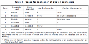 The failures usually showed up in the form of the devices resetting, or worse – a ‘permanent degradation of performance’ i.e. It fried something important.
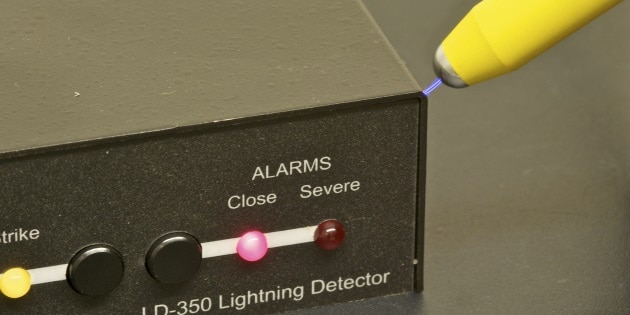
According to the adjacent table, taken from the root ESD testing standard (61000-4-2), ESD pulses are applied using the ‘contact discharge’ method to exposed metallic shells on connectors. These are usually connected to the PCB chassis ground through the connector. The amplitude of the discharge pulse depends on your product standard, but is typically 4kV or 8kV for most applications.
This is applied using a pointed tip as shown in the picture below.
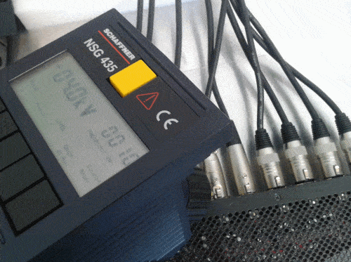
Here is a breakdown of several EMC design rules to avoid this very common issue:
Identify the ESD testing locations
In order to apply ESD protection to your product in the right places, you should know where the test lab is going to ‘zap’ it.
Unless stated otherwise in the generic, product-related or product-family standards, the
electrostatic discharges shall be applied only to those points and surfaces of the EUT which
are accessible to persons during normal use.
What this is saying is that if you can reach it with your finger, then it should be tested. The test lab will do some exploratory testing on the housing of your product to see if they can find any susceptible locations. If the chassis is non-conductive then often there won’t be many discharge points. Even on non-conductive chassis though, there are some common discharge points:
- Connectors
- Screw heads
- Buttons/Keypads
- Seams where two parts of the chassis come together
- Areas where internal PCBs come very close to the chassis
- LEDs or graphic displays
At 8kV or 16kV, the arcing distance can be quite far, so it’s possible for discharges to find a way to the circuit board, even through a non-conductive housing.
Identify the ESD levels
The ESD test levels are typically set by the product standard that applies to your product. For example, the consumer audio EMC immunity standard is EN55103-2, where the ESD test levels are defined as 8kV air discharge and 4kV contact discharge for almost all usage environments.
Select The right transient suppressor
Once you know the discharge test levels and where the discharges will be applied, you can proceed to selecting some ESD protection for your circuit boards. You can refer to section 4.6.1 from our EMC design guidelines eBook which goes into detail on these selections. There are plenty of options to choose from including spark gaps, resistors, capacitors, varistors and TVS diodes to name a few. A good ESD suppressor will clamp the maximum voltage seen across the device to a known level, and dissipate the extra energy into heat or noise.
Apply in the right location
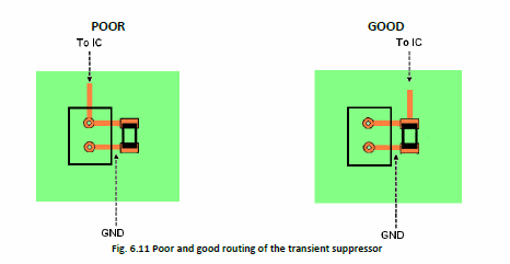 A critical aspect that is sometimes overlooked is the placement of the ESD protection. It must be placed as close as physically possible to area where the discharge event is going to happen. This minimizes the series inductance of any routing between the discharge location and the transient suppressor.
Design Your Discharge Path Properly
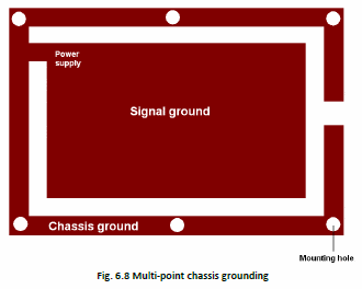 It’s important to visualize where the discharge path is for the discharges applied to a chassis ground on a connector. For many designs, the chassis ground is separated from the main board ground for safety reasons or even specifically for dealing with ESD.
A tried and tested methodology is to bring the chassis ground on your circuit board ground back to the main power input so that any discharges can dissipate through this point without affecting the rest of your circuitry.
3. EMC Design Tip #3 – Choose the right power adapter
If your product has an external power supply or internal sealed power converter, it’s very important to know how noisy these devices are. This can have a critical effect on your product’s conducted emissions performance. A $4 power supply can ultimately mean the difference between a pass or a fail at an EMC lab.
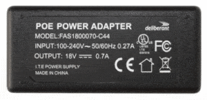
At the simplest level, you should ensure that the power adapter has passed the emissions class that your product needs to pass.
Class A digital devices are ones that are marketed exclusively for use in business, industrial and commercial environments.
Class B digital devices are ones that are marketed for use anywhere, including residential environments
Class B emissions limits are more strict than class A limits, so if your product is class B, then make sure that you’re using a class B power supply.
Unfortunately a compliant power adapter cannot guarantee that you’ll pass conducted emissions testing at an EMC lab. There are a couple of main reasons for this:
1. The emissions performance of a power adapter will likely have been tested at an EMC lab with only a DC resistive load connected to the output. It may well have passed class B emission limits with a DC load, but the emission characteristics of the adapter may be much different if it’s connected to a dynamic load with current supply requirements spread across a wide spectrum. A compliant power adapter can’t solve all of your conducted emission problems, you will also need to design your on-board power circuitry carefully to ensure that the RF current demands on the power adapter are minimized.
2. Power adapters are occasionally (ahem!) not as compliant as their labeling suggests. Giving the benefit of the doubt, some cheaper power adapter manufacturers suffer from quality control issues whereby some batches of adapters have worse emissions performance than the adapters they sent for testing at an EMC lab. A less trusting person might guess that some power supply manufacturers intentionally cost reduced their power adapter design after receiving their FCC or CE certificate. Or even worse, they may have acquired fraudulent test reports. But I’m not suggesting that.
It’s important that you request the test report from the power adapter manufacturer so that you can verify their claims. It’s also a good idea to provide your test lab with a couple of alternative samples of power adapter in case one of them is non-compliant.
4. EMC Design Tip #4 – All LCDs are not created equally
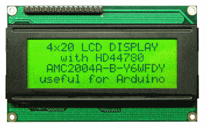 In the same way that your power adapter can have a big impact on your product’s conducted emissions performance, an LCD display can have a huge effect on your product’s radiated emissions performance.
Often an LCD will have a built in controller of some sort, with an integrated micro. Some LCDs can have much worse radiated emissions performance than a seemingly identical model from a different manufacturer.
It’s always a good idea to order some samples from several LCD manufacturers and either do an emissions pre-scan at a test lab or do some relative emissions measurements in-house if you have the right pre-compliance test gear. Usually there will be an identical drop in module from a different manufacturer available, so you can swap out an offending LCD if you run into issues. But if the LCD design is electrically or mechanically unique, this can be a really expensive and time consuming issue to fix.
As a side note, LCDs connected via a flex cable, or sometimes even via a DIP connector can exhibit significant radiated emissions due to the high slew rate digital signals. Follow the guidelines in point (1) above for implementing filters on the signals before they hit the connector/cable.
5. EMC Design Tip #5 – Make sure auxiliary equipment is compliant
Here’s how a $5 USB flash drive can cost your company $2000 and 1 week time to market.
It’s a bit unfortunate, but lots of manufacturers fail due to no fault of their own. As a general rule for emissions testing, manufacturers are required to connect auxiliary equipment to all I/O ports in order to fully exercise the functionality of their device. The FCC want to see worst case emissions profile, which involves exercising all interfaces and functionality.
For example, if the product includes a USB port that can connect to a USB flash drive in normal usage, then a USB flash drive must be provided with your equipment to your test lab. Surf on over to EBay and you’ll find that $5 can get you a no-name brand (possibly not FCC/CE compliant) 2GB flash drive, including shipping! At USB frequencies, a non-compliant device can cause you some really expensive headaches. You may spend hours debugging what you think is an emissions issue on your circuit board when it’s actually emissions emanating from a cheap USB flash drive. It may mean a trip back to your office and re-booking the test lab for a later date. All of a sudden, a $5 USB drive can cost you well over $2000 in extra expenses.
The rule of thumb here is easy:
Make sure that all auxiliary equipment that you supply to the test lab is from a reputable manufacturer so that you know it’s tested and compliant.
6. EMC Design Tip #6 – Select the correct rating of protection
It was very often the case that manufacturers had included transient protection circuitry, but had neglected to ensure that the rating of the devices were high enough to cope with the pulse that had to be applied.
I’ve included a table below of the normal ‘suite’ of transient disturbances that are applied to products during CE testing. I’ve also included some examples of test levels that may be applied. Note that this is from an old test report and the base standards and levels may not be up to date.
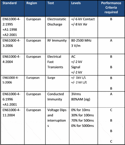
Selecting a transient device with a high enough rating to deal with the applied disturbances is critical to ensuring a first time pass. You need to be sure of the test levels that a test lab is going to apply to your product in order to know what type of protection you need to design in.
7. EMC Design Tip #7 – Shield any sensitive analog/RF circuitry
If your device contains any relatively sensitive analog circuitry, it’s a good idea to include a well grounded conductive shield. For CE testing, your product is more than likely going to be subjected to a radiated RF field in the 1 V/m to 10 V/m magnitude, modulated with a sine wave in the kHz region, swept over the frequency range 80 MHz – 6 GHz. It’s worth noting that some industries such as automotive, aerospace and military must design their products to a much higher specification and different types of modulation and sweep ranges are possible.
The energy in the RF field can couple to your circuit board in a number of ways, but in terms of pass/fail criteria, what you should be interested in is whether the field can negatively affect the performance of your device. Although traces on your circuit board may be electrically ‘short’ compared to the wavelength of the applied RF field, the field can still induce minuscule voltages/currents that can adversely affect the operation of your circuit. Sensors that provide current source outputs in the pA/nA can especially be affected. This typically shows up as a measurement error outside of the general specifications of the product.
Even non-analog parts of your circuit can be adversely affected by an applied RF field. For example, a very weak pull up resistor in the 1 M Ohm region on a static reset signal can be pulled below the ‘On’ threshold by an external RF field disturbance inducing a very small current on the signal. In terms of RF susceptibility, if design constraints allow you to avoid weak pull ups, it’s best to avoid them.
You might also be interested in:
- Getting EMC Design Right First Time – eBook
- The top EMC Failures and Tips from 5 EMC Consultants
- How to do an EMC Design Review
- The In-House EMC Test Equipment Guide
- Beginner’s Guide to EMC Testing
Wrap Up
In this post I’ve outlined the 7 most common causes of EMC failures I saw at my EMC lab over a 3 year period. Hopefully these tips can help you to avoid some seriously expensive failures.
If you’ve had a particular issue come up at a test lab, I’d love to hear what it was and how you solved it. Please send any questions or information to [email protected], or in the comments section below!

Comments 7
We had a problem with a switching power supply flooding an entire receiver with common-mode EMI. Solutions included placing a Faraday shield between the drain tabs of switching transistors and connecting them to their sources, including generous common-mode chokes between boards or LRUs connected by cables, changing to a push-pull converter v. a flyback, sealing LRUs with good shielding and using differential (victim) signal cabling / board traces wherever possible. Lesson learned was to design for EMC from the get-go. Another principle is “if it will hold water it will hold RF”, meaning that if an LRU (i.e., a box of electronics) is as hermetically tight to RF as possible, radiated and suscepted EMI is minimized.
Author
Ouch, sounds like a painful (and expensive) one! Definitely also advocate designing with EMC in mind from the get-go. Thanks for the story Robin.
I made a similar discovery to your cheap USB drive one. We have a video capture appliance, and have DVI inputs on it. In order to also capture HDMI and VGA (DVI-I) signals, we were using an adapter. I discovered that all of the adapters that we had did not have the shielding connected from one side to another, an thus were excellent RF emitters. I solved the problem by using cables that had one type of connector on one end, and the other type of connector on the other.
Our first pass with this product clearly showed how bad internal cables can be, especially the ones from the open frame PSU to the main board. Thanks for the article, it is excellent.
In your posting “Essential EMC Design Rules To Avoid The 7 Most Common EMC Failures” EMC Design Tip #2 – Connector Ground ESD you show in figure 6.8 you show chassis ground and signal ground are tied together. Any many other references from USB to Ethernet. They advise keeping chassis ground separate from digital ground planes to deny high voltage discharge paths to all of your digital circuit components. They advise instead of a direct connection an inductive one. There seems to be a lot of different ideas out there and Im not sure which is correct. I was hoping you could comment. Thank you in advance
Pingback: The top EMC Failures and Tips from 5 EMC Consultants - EMC FastPass
Hello Sir,
Thank you for your Valuable Suggestions. It could help us much while EMI/EMC product design.
I would like to ask one doubt that is How to ensure 360 degree shielding of Power, I/O cables.
Thanks in advance.
Very interesting post, Andy! Awareness is the first step toward electromagnetic compatibility. By considering electromagnetic emission and immunity as early as the idea and design stages, substantial alterations can be avoided later on. Before the actual engineering commences, an inventory of potential components or procedures susceptible to interference can be created. When inadequate EMC is discovered in the final stages, it frequently implies an expensive and time-consuming return to the drawing board.