
 In the world of electronic hardware design, achieving low electromagnetic interference (EMI) in printed circuit board (PCB) design is crucial.
By minimizing EMI, we not only stand a better chance of passing regulatory EMC testing requirements (such as the FCC, or CE Mark requirements), but we are also able to achieve higher data rates, lower crosstalk, higher accuracy measurements and cleaner signals.
This article delves into a nine-step process designed to streamline PCB designs for minimal EMI emissions. These steps are covered in detail in our 22-hour EMC Design for Compliance: Emissions online course.
By following these steps, engineers can significantly improve the electromagnetic compatibility (EMC) performance of their projects, ensuring that devices not only comply with regulatory standards but also deliver superior performance in a wide array of applications.
1. EMI-Friendly PCB Layer Stack-Up
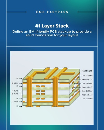 The foundation of any low-EMI PCB design begins with an optimal layer stack-up.
This step involves configuring the multiple layers of a PCB (such as signal, ground, and power planes) in a manner that inherently reduces EMI.
Strategic layer arrangement minimizes loop areas and enhances electromagnetic shielding, crucial for suppressing radiated emissions.
There are 6 important aspects to consider when designing an optimal EMC PCB stack:
- All signal layers should have an adjacent return plane (PWR or GND)
- Signal layers tightly coupled to a plane
- PWR + GND planes closely coupled (increased interplane capacitance)
- High speed signals on buried layers (to contain E-fields + shield critical signals)
- Multiple GND planes (to decrease return path inductance)
- Critical signals routed on max of 2 layers and referenced to same plane
It’s impossible to satisfy all 6 of these criteria with any less than an 8 layer board, so for a 4 layer PCB for example, we need to make some educated trade offs.
These aspects are covered in more detail in my “PCB Cost Reduction and EMC” article.
2. Component Zoning and Placement
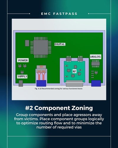 Once the PCB stackup has been defined, the next critical step in minimizing EMI is effective zoning and placement of components.
By segregating components based on their function and electromagnetic characteristics, designers can prevent high-speed signals from interfering with sensitive analog areas, thereby reducing noise coupling across different sections of the PCB.
Several strategies can be employed, which mostly involve keeping physical separation between aggressor and victim circuits.
When placing component groups, we need to consider 3 main electromagnetic coupling mechanisms including E-field (capacitive) coupling, H-field (inductive) coupling and conducted (common-impedance) coupling.
Generally we aim to keep noisy switching circuits such as DC-DC power supplies, and digital logic circuits away from more sensitive analog and RF circuits. We aim to minimize the crosstalk between any circuits or nets as much as possible by considering the 3 coupling mechanisms mentioned above.
3. Optimizing Connector Locations
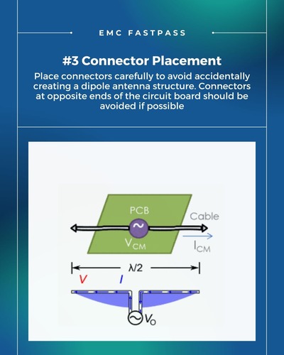 In the lower radiated emissions frequency range such as 30 MHz to a few hundred MHz, the dominant unintentional antenna structures are the cables attached to a product. That’s due to the physical length of a cable normally being the largest fraction of a wavelength of a noise source (such as noise on a ground plane).
If two connectors are placed at opposite ends of a circuit board, the problem is that if they share a noise conductor (such as a common ground wire) and a noise source (such as a switching IC) is located in between the connectors, then this can form an efficient dipole antenna structure.
In that case the noise can be efficiently radiated away from the PCB into the far-field, increasing the chances of exceeding the applicable radiated emissions limits.
For that reason it is preferable to keep connectors on one edge of a PCB only. This configuration makes it less likely that you’ll accidentally create an efficient dipole antenna structure that radiates noise unintentionally.
4. Place & Route Power Supplies
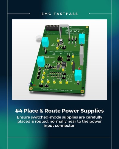 The next most critical aspect is to implement the power supplies on your circuit board.
DC-DC converters are probably the most common source of noise any given design (perhaps followed closely by LCD displays and processing ICs in general).
Placing the components optimally to minimize coupling and ringing is hyper critical if you want to control radiated and conducted emissions.
Some important aspects include:
- Consider input filtering (such as a basic L-C circuit)
- Place and route decoupling capacitors carefully to minimize important current loops
- Avoid accidentally creating resonant circuits
- Consider the placement and routing of the switching transistor carefully
- Consider the selection, placement and routing of the storage magnetic carefully
All of these factors (and more) are contributors to the magnitude of generated voltage and current noise.
In our EMC Design for Compliance: Emissions course, we cover these factors for many DC-DC topologies including buck, boost, flyback, LLC resonant converters and more.
Also check out the “DC-DC Converter Layout – Solid Ground Plane or Cutout Below Switch Node?!” and “SMPS Design for Low EMI (How to Pass Conducted Emissions Testing)” on our YouTube channel.
5. Place & Route Decoupling Capacitors
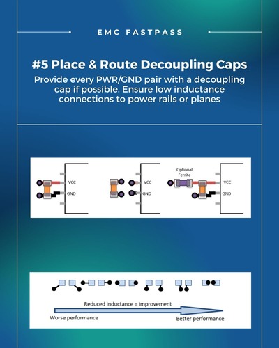
After the previous important steps have been taken care of, the next step is to place and route decoupling capacitors.
Optimal placement and routing of decoupling capacitors are crucial in electronic circuit design.
These capacitors serve as local energy storage at the point of use, providing a quick source of energy to the integrated circuits (ICs) during rapid transient loads and stabilizing the power supply voltage by filtering out noise and spikes.
An optimal placement, usually as close as possible to the power and ground pins of ICs, ensures that the path of least impedance is provided, significantly enhancing the effectiveness of the decoupling.
An alternative and equally acceptable option in the case where power and ground planes are available below an IC is to via directly to the planes from the capacitor as well as the IC pins. This can be a very low-inductance method to implement decoupling capacitors while allowing for physical separation of the capacitor on the IC.
By paying close attention to decoupling capacitor placement and routing, you can:
(a) Keep switching voltages/currents in a localized area
(b) Maintain a low PDN impedance across a broad range of frequencies
(c) Minimize radiated and conducted emissions
6. Applying Filters
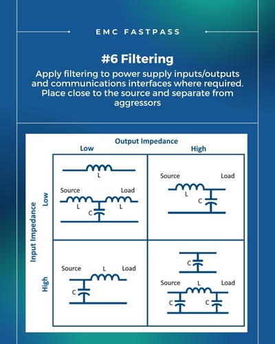 Filters, when implemented correctly, can be invaluable tools for localizing noise sources and suppressing unwanted frequencies.
Incorporating filters at critical points, such as power entry, signal interfaces, and IC power pin pairs, can significantly cut down on both conducted and radiated EMI.
As you can see from the graphic on the right hand side, different passive filter configurations are optimal for different combinations of the signal’s input and output impedance.
For example, where both the source driver to a filter circuit is high impedance, as well as the load impedance, then a shunt decoupling capacitor, or pi-filter circuit would be the best selections.
7. High-Speed Signal Routing
High-speed signals can be major contributors to EMI.
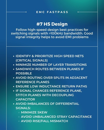
By ‘high-speed’ we’re not only referring to the main clock frequency of any switching signal, but also the rise and fall times.
Even a 100 kHz switching signal could be the source for an EMI failure because the harmonics of the signal can extend all the way up into the GHz region.
A 100 kHz signal could still have very fast rise and fall times, and a signal with high dV/dt can very effectively induce noise currents in adjacent conductors.
Sometimes the ‘high-speed’ signals of concern are referred to as ‘critical signals’, and there are a set of rules we can follow to maximize the chances that these signals will not be a problem in terms of EMI.
Additionally, by following these rules, you can also avoid signal integrity issues.
The image to the left outlines some of these best-practice guidelines:
(a) Identify & prioritize high speed nets (critical signals)
(b) Minimize number of layer transitions
(c) Sandwich routes between planes if possible
(d) Avoid routing over splits in adjacent reference planes
(e) Ensure low inductance return paths
(f) If signal changes reference plane, stitch planes with decoupling capacitor
(f) Avoid imbalances of differential signals:
(f)(i) Minimize skew
(f)(ii) Avoid unbalanced stray capacitance
(f)(iii) Avoid rise/fall mismatch
In the EMC Design for Compliance: Emissions online course we dedicate 4 hours to high-speed digital design.
8. Shielding
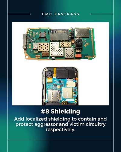 Good layout and routing practices can mitigate and localize a lot of noise issues, but in many scenarios where EMI cannot be adequately controlled through layout and routing alone, shielding becomes necessary.
Metal shields or conductive coatings can be employed to encase sensitive areas of the PCB, acting as a barrier against external electromagnetic fields.
They can also be used to protect sensitive circuits from external interference.
One important consideration when using shielding cans (as shown in the images to the right) is that they are generally only useful for E-field shielding (and sometimes H-field), but not for conductive (common-impedance) noise. That means that if a power rail, or ground rail is noisy, and it travels from outside to inside the shielded area, then it can very easily transport the noise past the shield.
So it is important to understand what type of noise you’re trying to mitigate by using a shield.
Another often forgotten aspect is that copper tracks that traverse the shield boundary on an internal or external PCB layer can also be effective at transporting EMI past a shield. For that reason, designers often aim to filter all signals that are routed from inside to outside the shield.
Shielding can be very effective, but it is never a good idea to rely on a shield to solve all EMI issues. This is very often not a viable solution and the best idea is always to use best practices for PCB design and layout, and use shielding as a backup or an additional layer of protection.
9. Impedance Control
The last important step in this process is to consider and define an impedance control chart on a fabrication document.
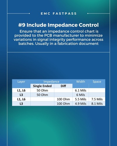
Maintaining consistent impedance across transmission lines minimizes signal reflections and reduces EMI. For example the USB 2.0 specification calls for a 90 Ohm differential impedance. By carefully defining the USB track widths, gap, and height about the reference plane, the signals impedance can be set to a reasonable tolerance. But if this information is not communicated clearly to the fabrication house, then you may see significant batch-to-batch variations in terms of signal integrity and EMI.
That is why we always want to see the layer stackup and controlled impedance track geometry defined in a fabrication document.
Conclusion
 By carefully applying the nine-step process outlined above, engineers can significantly mitigate EMI in their PCB designs. This approach not only facilitates compliance with EMC regulations but also enhances the overall performance and reliability of electronic devices.
As data rates continue to increase and electronic devices become increasingly interconnected, the importance of EMI-conscious design becomes even more important as well as challenging.
This process, tailored for practical applications, offers a comprehensive blueprint for engineers aiming to master the challenges of EMC in PCB design.
Comments 1
This information it’s very useful for us as an E-Mobility engineer.