
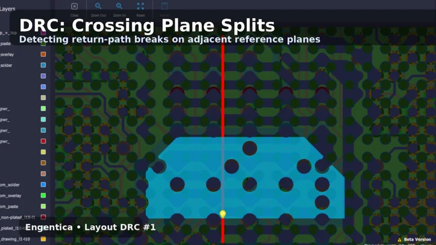
First spatial-geometry PCB layout DRC is running in Engentica.
It flags signals that cross a split in an adjacent reference plane.
Why this matters
Return current wants to flow right under the trace. A plane gap forces it to detour → loop area increases → more radiation (and higher return-path inductance).
This isn’t theoretical. I’ve demo’d this effect with a near-field probe: you can see the hot spot right over the gap.
The nuances
The nuances matter though.
If one plane is closer, return current disproportionately prefers that layer. Single-sided reference behaves differently than stripline. And not every signal matters – a rough rule is f>10kHz (although it’s the slew rate that really matters).
Why Engentica is different
Most rule checkers spam hundreds of warnings. Because Engentica has schematic + layout context, we will flag only the nets that actually matter – and tell you why.
(We’re building this in stages. The spatial geometry engine is working. Context filtering comes next. One step at a time.)
What this represents
Building the underlying spatial geometry engine took real work. Now it’s in place, we can scale the DRC library.
More DRCs coming.